Product Summary
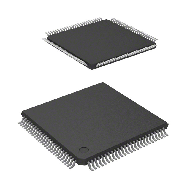
The A3P125-VQG100 is a proasic3 flash family FPGA. A3P125-VQG100, the third-generation family of Actel flash FPGAs, offers performance, density, and features beyond those of the A3P125-VQG100 family. Nonvolatile flash technology gives A3P125-VQG100 devices the advantage of being a secure, low-power, single-chip solution that is live at power-up (LAPU). A3P125-VQG100 is reprogrammable and offers time-to-market benefits at an ASIC-level unit cost. These features enable designers to create high-density systems using existing ASIC or FPGA design flows and tools. A3P125-VQG100 devices offer 1 kbit of on-chip, reprogrammable, nonvolatile FlashROM storage as well as clock conditioning circuitry based on an integrated phase-locked loop (PLL). The A3P125-VQG100 device has no PLL or RAM support. ProASIC3 devices have up to 1 million system gates, supported with up to 144 kbits of true dual-port SRAM and up to 300 user I/Os. A3P125-VQG100 device supports the ARM7 soft IP core and Cortex-M1 devices. The ARM-enabled devices have Actel ordering numbers that begin with M7A3P (CoreMP7) and M1A3P (Cortex-M1) and do not support AES decryption.
Parametrics
A3P125-VQG100 absolute maximum ratings: (1)VCC DC core supply voltage: –0.3 to 1.65 V; (2)VJTAG JTAG DC voltage: –0.3 to 3.75 V; (3)VPUMP Programming voltage: –0.3 to 3.75 V; (4)VCCPLL Analog power supply (PLL): –0.3 to 1.65 V; (5)VCCI DC I/O output buffer supply voltage: –0.3 to 3.75 V; (6)VMV DC I/O input buffer supply voltage: –0.3 to 3.75 V; (7)TSTG2 Storage temperature: –65 to +150 °C; (8)TJ2 Junction temperature: +125 °C.
Features
A3P125-VQG100 features: (1)High Capacity: 15 k to 1 M System Gates, Up to 144 kbits of True Dual-Port SRAM, Up to 300 User I/Os; (2)Reprogrammable Flash Technology: 130-nm, 7-Layer Metal (6 Copper), Flash-Based CMOS Process, Live at Power-Up (LAPU)Level 0 Support, Single-Chip Solution, Retains Programmed Design when Powered Off; (3)High Performance: 350 MHz System Performance, 3.3 V, 66 MHz 64-Bit PCI+; (4)In-System Programming (ISP)and Security: Secure ISP Using On-Chip 128-Bit Advanced Encryption Standard (AES)Decryption (except ARM-enabled ProASIC®3 devices)via JTAG (IEEE 1532–compliant)+, FlashLock® to Secure FPGA Contents; (5)Low Power: Core Voltage for Low Power, Support for 1.5 V-Only Systems, Low-Impedance Flash Switches; (6)High-Performance Routing Hierarchy: Segmented, Hierarchical Routing and Clock Structur.
Diagrams

| Image | Part No | Mfg | Description |  |
Pricing (USD) |
Quantity | ||||||||||||||||||||||
|---|---|---|---|---|---|---|---|---|---|---|---|---|---|---|---|---|---|---|---|---|---|---|---|---|---|---|---|---|
 |
 A3P125-VQG100 |
 |
 IC FPGA 1024MAC 133I/O 100VQFP |
 Data Sheet |

|
|
||||||||||||||||||||||
 |
 A3P125-VQG100I |
 |
 IC FPGA 1KB FLASH 125K 100-VQFP |
 Data Sheet |

|
|
||||||||||||||||||||||
 |
 A3P125-VQG100T |
 |
 IC FPGA 1KB FLASH 125K 100-VQFP |
 Data Sheet |

|
|
||||||||||||||||||||||
 (China (Mainland))


